
Chiplets: the future of semiconductor IP
Tiny chiplets, big dreams.

It takes a village to make a chip. First of all, a complex chip project involves a massive team of architects, digital designers, verification engineers, and physical design engineers. But even with all those engineers, companies can’t develop their chips alone; to build a project as complex as a modern chip, most companies have to purchase large parts of their designs from third parties.
Logically, this makes sense; as a chip company, you want to focus on your unique and differentiated technology, rather than building a standardized memory interface controller from scratch. So companies buy third-party designs, called IP blocks, that can do everything from encrypting data, to communicating with off-chip memories, to encoding and decoding video streams. Then, these companies use these third-party designs as key building blocks in their chips. An entire industry of IP block licensing has grown over the years, and you’ve probably heard of some of the big names, like ARM and Syopsys.
But there’s an issue with the IP licensing business model. Unless you’re one of the biggest players in the space, like ARM, it’s not very lucrative. Most IP vendors end up having to sell their IP for a flat, upfront price with no royalties, so they make the same amount of money whether the end product sells 10 units or 10 million units. This makes IP vendors unattractive venture investments, and means that they often can’t scale past a small number of simple IP products.
However, in the next decade or so, there’s going to be a major change in the world of silicon IP. That change is going to be chiplets. By selling small, pre-built chiplets that get packaged into a larger chip, IP vendors can capture more value and scale more efficiently than they ever could before. They may even become exciting investments for venture capitalists! But to understand why chiplets are the future, we have to first understand the problems faced in the traditional IP business model.
Why is the IP business so hard?
At a high level, there are two kinds of IP that a vendor can sell: hard IP and soft IP. Soft IP is fairly similar to software; as a vendor, you design a piece of digital logic using a Hardware Description Language (HDL) like Verilog, and then you license that logic design to customers. The customer is responsible for taking your logic, integrating it into their system, and taking it through the physical design flow that maps your logic down to actual transistors on the chip. This limits a vendor’s ability to capture all of the value their designs create; each customer needs to do that physical design work themselves, so they end up less willing to pay their IP vendors. At the same time, because soft IP vendors don’t have to perform difficult physical design work, the barrier to entry for soft IP vendors is lowered. This increases competition and further drives down prices.
What if the vendor wants to capture all of the value they could by delivering fully laid-out and tested IP? This is what we call hard IP -- the deliverable to customers is an actual transistor-level layout of the design. However, that layout needs to be different for every single process node from every single fab. The layout you’d need to provide for Intel’s 65nm process and TSMC’s 5nm process would be wildly different. To support all possible customers with hard IP, a vendor needs to expend significant resources delivering their IP in every process node that might need it. While some vendors execute on this strategy successfully, it limits their ability to scale quickly and affordably to many customers.
What is a chiplet?
For decades, if you wanted to put multiple subsystems on a chip, you had to design them all together, on one single die of silicon. Your CPU, security subsystem, floating-point unit, and all other features you wanted on your chip would all be designed together, laid out together, and manufactured together. But as modern chip manufacturing got more and more expensive, people started to wonder: what if we could design parts of the chip in one manufacturing process, and different parts of the chip in a different manufacturing process?
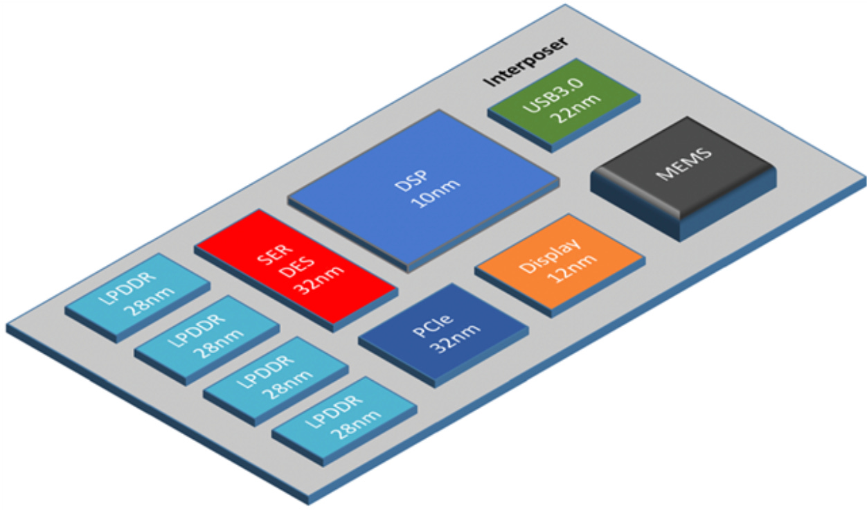
This has a number of advantages. You only need to use the expensive, advanced manufacturing processes for subsystems that benefit from them. Plus, your system has improved manufacturing yield. Normally, if you have a fault in one subsystem of a chip, you have to replace the entire die. But with a chiplet-based design, if any chiplet has faults, it can be discarded and replaced with a tested, known-good chiplet.
For example, if you’re designing a microcontroller with an AI subsystem, you could design an AI accelerator in a more advanced process node than the host microcontroller. As a matter of fact, that’s exactly what Femtosense’s new AI-ADAM100 did! And if you wanted to add a radio subsystem, you could design it in a process node optimized for radio-frequency circuits. Ultimately, chiplets give system designers greater flexibility while also lowering system cost.
So why aren’t chiplets more common? There are two main reasons: packaging technology, and the availability of off-the-shelf chiplets for designers. And both are getting solved right now.
The chiplet revolution is coming.
In the past, it was nontrivial to physically package many different small chiplets into one package. But advances in packaging technology, spurred on by the desire to make ever-bigger AI chips, have made chiplet packaging easier and more cost-effective. In 2022, the Universal Chiplet Interconnect Express (UCIe) standard was released, followed by the Bunch of Wires standard in early 2023. These standards and packaging technologies make it easier than ever to build a system that leverages chiplets to their full potential.
But building a practical system out of chiplets also requires an ecosystem of chiplet providers, selling chiplets for systems integrators to purchase and leverage. This ecosystem is in its infancy, but it’s getting there. Like I mentioned earlier, Femtosense is selling ultra-low-power AI chiplets for embedded devices, but they’re not the only chiplet provider in the game. AyarLabs sells photonic interface chiplets, AlphaWave sells DDR5 controller chiplets, while Tenstorrent is working on high-performance AI chiplets.
All of these startups are excited about chiplets for a simple reason: they solve the problems that conventional IP business models have. Like hard IP, a chiplet provider gets to deliver a complete, functional, tested silicon design, which enables them to charge higher prices. But unlike hard IP, a chiplet provider only needs to implement their design in a single process node, significantly reducing the manpower required and increasing the scalability of the end product. A chiplet combines the best of both worlds: a vendor can reach as many customers as they would with soft IP, but can capture the same amount of value as they would for hard IP. And because chiplets are sold as individual units with a manufacturing cost, vendors don’t have to fight tooth-and-nail for IP royalties. It’s natural for systems manufacturers to pay per-chiplet.
For decades, venture capitalists have shied away from investing in semiconductor IP vendors because of the limitations they would face selling either hard IP or soft IP. But now, with the chiplet business model, a new slate of high-margin, scalable chiplet startups will spring up to support the ecosystem of systems integrators building with chiplets. Here’s my prediction for all the VCs out there: the chiplet revolution is coming!